The Institute of Micro- and Nanostructure Research together with CENEM own three transmission electron microscopes (TEM) with various TEM specimen holders, a scanning electron microscope (SEM), a scanning electron microscope / focused ion beam SEM/FIB Dualbeam System and a broadly equipped sample preparation laboratory. With the expertise of the staff and this equipment high-end research can be performed in the huge field of electron microscopy. Detailed information about the various TEM, their accessories, the sample preparation as well as the FIB can be found below.
Transmission Electron Microscopes
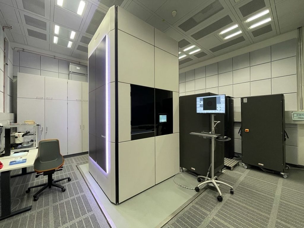
The Titan Themis3 300 is one of our two high-end TEM providing high-resolution imaging as well as high performance analytical investigation capabilities. This double-aberration-corrected TEM corrects both the image and the probe forming system enabling high-resolution imaging in TEM as well as scanning TEM (STEM) mode resulting in resolution limits below 1 Å for both modes for all high tensions between 60 kV and 300 kV. The high brightness electron gun (X-FEG) equipped with a monochromator to improve the energy resolution in combination with a high-sensitivity SDD X-ray spectrometer (Super-X) and a high-resolution post-column energy filter (GIF Quantum) creates a high performance analytical instrument perfectly suited for the nanoanalytical characterization of all kinds of materials and devices. Energy filtered TEM (EFTEM) imaging, high-resolution electron energy-loss spectroscopy (EELS) as well as energy-dispersive X-ray spectroscopy (EDXS) yield chemical, elemental as well as bonding information even down to the atomic scale. Additionally information about local band gaps and plasmonics are gained by monochromated low-loss EELS investigations. Furthermore, the Titan Themis3 300 is used to perform advanced in situ experiments using special TEM specimen holders. A further advanced method available at the Titan Themis3 300 is electron tomography enabling the analytical characterization of materials and devices in 3 dimensions. This high-end analytical TEM is used to answer the most complex questions regarding materials science.
- Emitter X-FEG
- High tension: 60-300 kV
- Monochromator, energy resolution 0.2 eV
- Cs probe corrector (CEOS, DCOR)
- Image-side Cs corrector (CEOS, CESCOR)
- Gatan imaging filter (GIF Quantum)
- HAADF detector for Z-contrast (Fishione)
- ADF/ABF/BF detectors (FEI)
- Videocamera (Flucam)
- 4k CMOS camera (Ceta 16M)
- High-efficiency Super-X detector (EDX)
- Tomography sample holder and software
- Special TEM holders (see below)
The Spectra 200 provides high-resolution imaging as well as high-performance analytical investigation capabilities. This probe-corrected TEM enables high-resolution imaging in scanning TEM (STEM) mode for all high tensions between 30 kV and 200 kV. The ultra-high-brightness cold field emission gun (X-CFEG) with an energy resolution of < 0.4 eV in combination with a high-sensitivity SDD X-ray spectrometer (Super-X) and a high-resolution post-column energy loss spectrometer (Gatan Continuum S) creates a high-performance analytical instrument perfectly suited for the nanoanalytical characterization of all kinds of materials and devices. High-resolution electron energy-loss spectroscopy (EELS) as well as energy-dispersive X-ray spectroscopy (EDXS) yield chemical, elemental as well as bonding information even down to the atomic scale. Furthermore, the Spectra with its Ceta-S 4k high speed CMOS camera (up to 400 fps at binning 512) is used to perform advanced in situ experiments by making use of special TEM specimen holders available at CENEM. Moreover, in combination with simultaneous STEM imaging, the Spectra 200 allows for 4D-STEM investigations. A further advanced method available at the Spectra 200 is electron tomography enabling the analytical characterization of materials in three dimensions. This high-end analytical TEM enables to answer the most complex questions in almost all discipline of materials science and nanotechnology.
The most important specifications of the TFS Spectra 200 are:
- X-CFEG emitter
- High tension: 30-200kV
- Energy resolution < 0.4 eV
- Probe Cs corrector (CEOS S-CORR)
- Point resolution for STEM: 60 pm @ 200 kV, 125 pm @ 30 kV
- Gatan spectrometer (Gatan Continuum S)
- Super-X detector G2 (EDXS)
- BF, ADF STEM and iDPC imaging: 8 segmented BF and ADF detectors (16 segments in total)
- 4k CMOS camera
- Electron tomography functionality (including EDXS)
The Philips CM30 TEM/STEM is used for several in situ experiments to investigate on the one hand temperature dependent properties and mechanisms by heating and cooling experiments and on the other hand to investigate elastic and plastic properties by nanomechanical testing. Furthermore advanced conventional techniques are performed on the CM30 like e.g. large angle convergent beam electron diffraction (LACBED) for crystallographic analyses. For high contrast applications the imaging plates are used to obtain improved diffraction patterns.
- LaB6 cathode
- High tension: 150-300kV
- Twin objective lens (Cs = 2 mm)
- Point resolution (Scherzer): 0.23 nm
- 1k x 1k CCD camera (Tietz FastScan-F114)
- EDXS detector (Oxford)
- CL system (Oxford)
- Imaging Plates
Scanning Electron Microscopes & Focused Ion Beam SEM/FIB Dualbeam systems
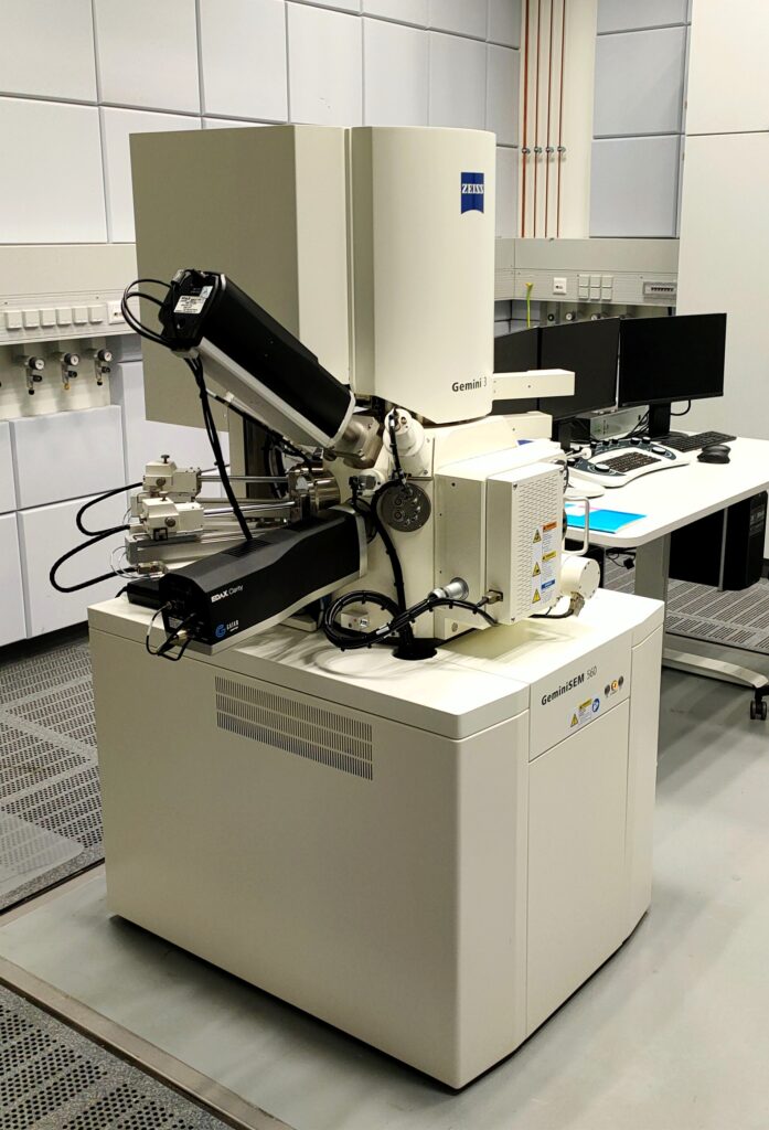
The microscope is ideally suited for low-dose, low-kV, and reduced-pressure operation for high-resolution SE/BSE/STEM imaging, electron backscattered diffraction (EBSD), energy-dispersive X-ray spectroscopy (EDXS), and transmission diffraction (TD) analysis on nanomaterials, beam sensitive-, non-conductive and magnetic samples. Highlights are in particular an ultra-sensitive direct detection camera for EBSD (Clarity Super, Ametek) and a customized setup consisting of an ultrafast direct detection camera (Timepix 3) combined with a flexible hexapod sample stage (SmarAct) for TD. This dedicated equipment enables optimized crystal structure and orientation analysis of beam sensitive nanomaterials. The TD setup is currently under development and expected to be operational within the next month.
- High-resolution electron column (Zeiss Gemini 3) with Schottky emitter and immersion-free optics
- Resolution: 0.5 nm at 15 kV, 1.0 nm at 0.5 kV
- Flexible and continuous tuning of acceleration voltage (0.02 – 30 kV) and beam current (3 pA – 20 nA)
- Sample biasing to improve resolution at low landing energies (0.7 nm at 1 kV landing energy)
- High-resolution In-lens detectors for SE and energy-selective BSE detection (EsB)
- Retractable 6-segment BSE detector with simultaneous measurement of up to 4 signals
- Retractable 7-segment STEM detector with simultaneous measurement of up to 4 signals
- Direct detection EBSD camera (Clarity Super, Ametek GmbH) with excellent low-kV (~3 kV) and low dose (<10 pA) performance, zero read out noise and distortion, single-electron sensitivity and high dynamic range
- Fast EDXS detector (Octane Elite Super, Ametek GmbH): Silicon Drift detector (SSD) with large detection area (70 mm²), high sensitivity for detecting low energy signals (e.g. Al L at 73 eV), good energy resolution (Mn Kα: 123 eV) and high throughput count rate (limit: 850k output cps at 2.0m input cps).
- Low vacuum mode (10 to 500 Pa) enabling simultaneous usage of high-resolution Inlens detectors (in conjunction with beam sleeves) up to 150 Pa (resolution: 1.0 nm at chamber pressure of 30Pa and 15 kV, 0.4 nm at chamber pressure of 30 Pa and 3 kV)
- Eucentric 6-axis sample stage
- Automatic load lock (80 mm)
- In chamber plasma cleaner
- Customized TD setup (under development) consisting of a hexapod stage (SmarAct GmbH) with eucentric tilt for precise and flexible sample positioning and an ultrafast direct detection camera (Timepix 3)
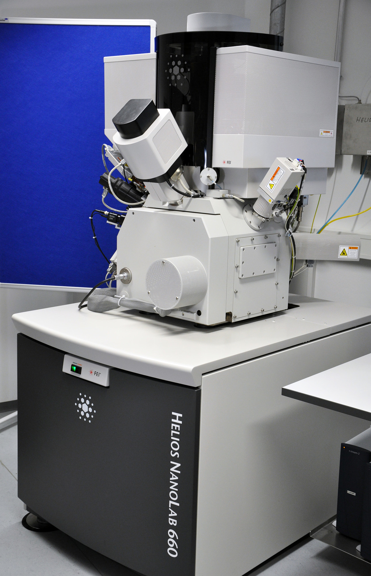
The FEI Helios NanoLab 660 Dualbeam System combines ultra-high resolution SEM imaging with extremely precise FIB milling. Having 8 different detectors, the instrument is capable of resolving a large variety of signals like secondary electrons, x-rays, and secondary ions. Using the Ga-ion FIB material can be removed with nanometer precision to prepare site-specific cross-sections, TEM lamellae or structures for mechanical tests. Three different gas injection systems are available that can be used for different purposes. Carbon and Platinum can be deposited in order to protect a surface or to do circuit editing, while XeF2 can be used for ion-less milling of certain materials. In addition Two micro-manipulators are available for lift-out procedures, sample transfers and mechanical or electrical probing.
- Ultra-high resolution ElstarTM electron column with monochromator
- Resolution ~1 nm at 1-30 kV
- Retractable STEM and different SE & BSE detectors for advanced imaging contrasts
- High-resolution TomahawkTM ion column
- Gas Injection System for Pt, C and XeF2
- EasyLift NanoManipulator
- Kleindiek micromanipulator
- Oxford X-MaxN EDX detector (150 mm2 SDD)
- Oxford Instruments EBSD detector
- Gatan heating stage
- In-chamber plasma cleaner
TEM specimen holders
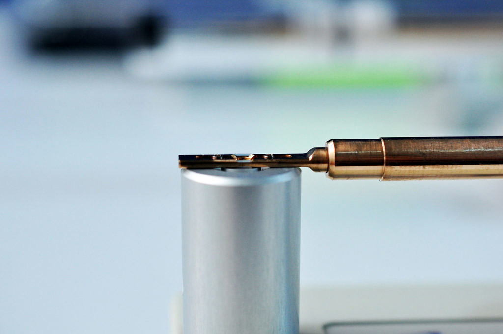
Several TEM specimen holders are available to enable a variety of different experiments. Several single tilt, double tilt and rotation holders allow any orientation of the specimen inside the TEM. A vacuum transfer holder can be used for specimens sensitive to ambient air. Cooling and heating holders enable the investigation of temperature dependent properties and mechanisms like e.g. phase transitions. The MEMS based heating holders improve the performance of the TEM investigation as only a minimum area of the holder is heated controlled. The cooling holder can be used for beam sensitive specimens to improve specimen stability. For electron tomographic investigations two tomography holders are available. The 360° tomography holder enables reconstructions without the missing wedge artifact. Special in situ holders like the PicoIndenter, the TEM-STM and TEM-AFM holders enable advanced in situ investigations regarding nanomechanical testing, force measurements as well as measurements of the electrical properties.
- Single tilt holders (FEI/TFS)
- Double tilt holders (FEI/TFS)
- Rotation holder (Philips)
- Vacuum transfer holder (Gatan)
- LN2 cooling holder (Gatan)
- Cryo-Tomography LN2 cooling holder (Fischione)
- Helium cooling holder (-253 °C)
- Single tilt heating holder, MEMS based (DENSsolutions)
- Double tilt heating holder, MEMS based (DENSsolutions)
- Tomography heating holder, MEMS based (DENSsolutions)
- Single-Tilt Tomography holder (FEI/TFS)
- Single-Tilt EDXS tomography holder (FEI/TFS)
- 360° Tomography holder (Fishione)
- Dual-axis rotation tomography holder (Fischione)
- PI 95 TEM PicoIndenter (Hysitron)
- TEM-STMTM holder (Nanofactory)
- TEM-AFMTM holder (Nanofactory)
Sample Preparation
As the quality of the sample is a crucial and important factor for the TEM investigation, several different machines are available for the wide range of user needs regarding the sample preparation. Mechanical methods like grinding, dimpling and polishing can be used for bulk material removal and geometrically precise polishing techniques. Ion beam instruments offer final milling as well as cleaning methods. Soft materials can be prepared in the cryo-ultramicrotome either at ambient or at cryo-temperatures. Additional equipment like wire saws, coating machines, evaporators, spin coater, ovens are available as well as a glove box, a plasma cleaner and various light microscopes.
- 1 Ion Polishing Systems (Gatan PIPS II with low-energy ion guns and LN2 cooling)
- Various grinding machines (Struers LaboPol-21, Buehler EcoMet30)
- Semiautomatic polishing machine (Allied Multiprep)
- Low volume semi-automatic polisher (Buehler Minimet 1000)
- 2 Wire Saws (Well model 3400 and 3242)
- Precision cutter (Buehler Isomet1000)
- 2 Dimpling machines (Gatan model 656)
- Ultrasonic cutter (Gatan model 601)
- Coating machines (Korvus HEX Base 300, Baltec Med 020)
- Carbon Coater (Leica EM ACE200)
- Evaporators
- Spin coater (Laurell WS650Mz-23NPP)
- Automatic film applicator (Zehntner ZAA 2300)
- Cryo-ultramicrotome (Leica EM UC6)
- Different ovens (Binder VD53, Gero HTRH 40-250/16, Gero SR 100-650)
- Various light microscopes (Zeiss, Nikon)
- Stereo microscopes (Leica M205C, M80, S9)
- Plasma Cleaners (Fishione Model 1020 and Model 1070)
- Glove Box (GS T3)
- Tabletop ultra-centrifuge (Hermle Z36HK)
- Analytical balance (Mettler-Toledo XS204DR)
- Precision balance (Kern & Sohn PBJ 4200-2M)
- Vitrobot (FEI Vitrobot MarkIV)