Home
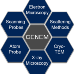
The Center for Nanoanalysis and Electron Microscopy (CENEM) is a facility featuring cutting-edge instrumentation, techniques and expertise required for microscopic and analytical characterization of materials and devices down to the atomic scale. CENEM focuses on several complementary analysis techniques, which closely work together: Electron Microscopy, X-ray Microscopy, Cryo-TEM, Scattering Methods, Scanning Probes and Atom Probe Microscopy.
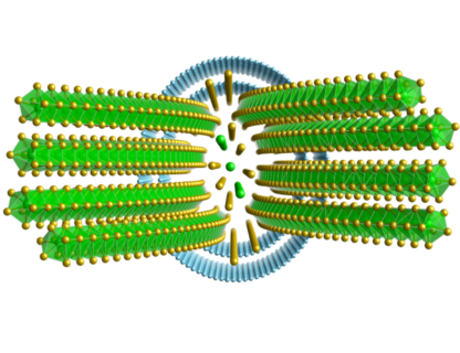
In a milestone study, CENEM and IMN scientists have demonstrated a novel technique that uncovers the three-dimensional structures of nanomaterials, including those made of light elements that have eluded detection until now. This advance, which utilizes ptychographic electron tomography, showcases a...
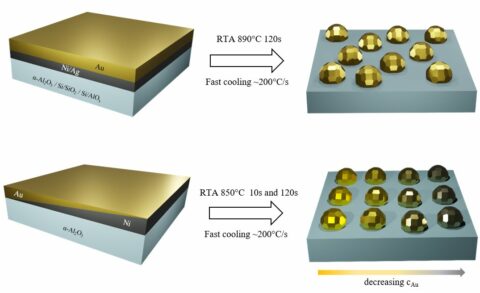
The paper “Influence of Au alloying on solid state dewetting kinetics and texture evolution of Ag and Ni thin films” by Martin Dierner, Johannes Will, Michael Landes, Christian Volland, Robert Branscheid, Tobias Zech, Tobias Unruh and Erdmann Spiecker has just been published in the Journal of Surfac...
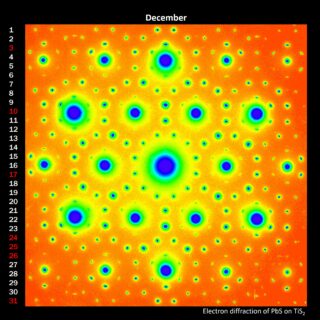
Just in time for Advent, the stars arrange themselves in a highly symmetrical pattern.
The beautiful picture was actually created using electron diffraction, with the electron beam transmitting through a thin PbS film grown epitaxially on a TiS2 substrate. While the six-fold symmetry of the substr...
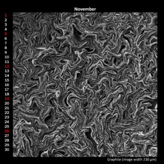
Graphite, a versatile material. On the one hand it is used in daily life as pencil, on the other hand graphene with its remarkable properties can be produced by cleaving graphite. This scanning electron microcopy image shows the beautiful structure of graphite, which consists of only one element, ca...
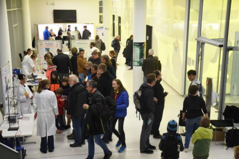
During the Lange Nacht der Wissenschaften (LNdW) 2023 on October 21, we demonstrated how microcopy enables us to decipher the building blocks of the universe, and how this helps to understand and develop new energy materials with enhanced properties. We showcased the application of modern electron a...